9th March 1995
H1 Silicon Trackers DAQ
A Guide to Front-End Hardware Configuration and Mac-based Software Utilities
G. W. Noyes
Rutherford Appleton Laboratory
DISCLAIMER
The author makes no warranties, express or implied, that the examples, data, or other information in this document are free of error, that they are consistent with industry standard, or that they will meet the requirements of any particular application.
Independent testing and verification are especially important in any application in which incorrect functioning could result in personal injury or damage to property.
The following section is intended as a reference for the hardware and software configuration of the key components of the H1 Silicon Data Acquisition branch[+]. Some of the information contained in this note is taken from the hardware documentation of the components, but is collated here for quick reference. This note also includes some discussion of the concepts of the data acquisition philosophy with particular regard to the readout sequence. For a broader overview of the silicon tracker data acquisition architecture and protocols, refer to [1].
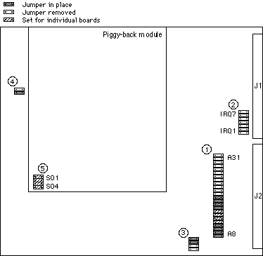
1) Module address (p29)
The base address of the OnSiRoCs is set at $Fx'0000 in A24 address space (jumpers A20-A31 removed, A8-A15 in place), where x denotes the module number. By convention the left-most OnSiRoC in a crate is module number 0, increasing to the right to a maximum of 16 OnSiRoCs in a crate. The module number must therefore be set according to the position in the crate, using jumpers A12-A15 (removed = high). Note that for OnSiRoCs in custom OnSiRoC crates (as in H1), geographical addressing is implemented via a custom backplane, thus removing the need for jumpering the module address.
2) VME interrupt signals enable/disable (p32)
All jumpers should be disabled, as interrupts are not presently used. Instead the status registers of the OnSiRoCs are polled. Top jumper is IRQ7.
3) STC Clock divider (p26)
Default jumper positions: top two jumpers in place (2.5 MHz). Ultimate jumper position will depend on the clock speed required to drive the APC for readout. The standard scan frequency (10 MHz) is unaffected. The divider works as follows: insert jumpers such that binary representation is n (top jumper = bit-0, bottom = bit-3). The slow sequencer frequency (toggled with SQD 8) is then F(10,n + 1) MHz.
4) Sequencer front-panel control signals enable/disable (p18)
Overrides CSEn* for front-panel signals. Front-panel control signals are a useful way of cross-checking the functioning of the OnSiRoC, sequencer and APC, and should therefore always be enabled. Note that if a signal is fed into the Cosmic Stop connector on the front panel, the sequencer will automatically start reading out an event irrespective of whether the control signals are enabled or disabled.
5) Analogue monitor output to front-panel (p39)
Select which analogue channel is output to front panel. Top jumper is S01. Signals are the analogue outputs after fine and coarse pedestal subtraction, if enabled (see p2, 3 and control register 2).
The following can be set, but have been hardwired in the production OnSiRoCs, so each will be the same:
* Sequencer clock delays (p15)
* Clock phase shifter (p17)
* Raw memory WE (p21)
Figure 1: default jumper settings for OnSiRoCs in the H1 silicon branch. The numbers refer to the items in section 1.1.
* PEn*. Pedestals enable (p2, 3). Enables the pedestal DAC (active low).
* ClkInt. Internal clock (p26). Determines whether the clock is generated locally, or whether it is taken from the backplane. Note that the backplane HCk is driven by the STC Interface card from the STC-distributed clock.
* PIOn. Pipeline on (p26). Forces the pipeline enabled signal, whether the STC condition is true or not.
* PIOff. Pipeline off (p26). Disables the externally driven pipeline enabled signal.
* FCOff. Fast clear off (p26). Disables the externally driven fast clear signal.
* FEREn*. Front-end-ready enable (p26). Allows the front-end-ready signal to be broadcast onto the backplane (active low). This signal is detected by the STC Interface card, which then sets the FER signal on the STC fast card.
* L2Off. Level-2 off (p26). Disables the externally driven level-2 keep signal.
* L2Auto. Allows the automatic handling of the trigger sequence. In practise this means that sequencer start address 2 is automatically invoked on receipt of a L2K signal, and that FER is generated at the end of the sequence when SQD15 is set. The sequencer start address 1 is also invoked on receipt of a fast clear signal.
* CSEn*. Control signals enable (p18). Allows the sequencer bits to be driven to the front-end. Note that although 16 bits are controlled by the sequencer, only bits 0-3 are sent to the decoder and APC.
* IRMod1, 2. Signals used to encode the VMEbus interrupt level (0,0 = no interrupts; 1,0 = levels 2-3...)
* IRD0-4. Used to generate interrupt vectors.
CAUTION: the signals set in this register affect the operation of the OnSiRoC. Be sure to initialise this register after switching on the card. Beware of the unpredictable effect of uninitialised counters and undefined code in the sequencer.
Signals SITP1-4 are used to disable the inward analogue signals (1 = disable), so that only the pedestals undergo digital-to-analogue conversion. This is for test purposes only (p2, 3).
* ClkOn. Sequencer Clock on (p15). Indicates that the sequencer is in operation.
* PIOn. Pipeline on (p26). Pipelines are running. The OnSiRoC should therefore be in scan-mode.
* L2POn. Level-2 prompt on (p26). A L2K signal is still pending.
* L2DOn. Level-2 delay on (p26). Flip-flop used to guard against reading out a second event before the first has been read-out of the raw-data memories. If this bit is set, the OnSiRoC has started to readout an event, and may even have finished. Under normal circumstances, once the front-end readout has finished, the sequencer will also have set FERDisp* (see below). The flip-flop must be reset by writing to the L2-delay reset register (offset $7C) once an event has been read-out from the output memories.
* FERDisp*. Front-end ready on (p26). Inidcates whether the OnSiRoC readout sequence has finished. Note that in practise this is set by the sequencer bit SQD15 when L2Auto is enabled in control register 1.
* ADRdy. ADC ready (p63). The analogue-to-digital conversion is finshed.
* IROn. Interrupt On (p32). An interrupt has been set, but not acknowledged. Note that VME interrupts do not have to be enabled for the status register to reflect this bit. Interrupts are cleared by writing to the L2-delay reset register.
Note that for 'normal' operation the sequencer should be programmed with at least two routines. The first is invoked on receipt of a fast clear signal and sets up the card and APC for running. The end of the set-up phase is signalled by generating SQD13. The second routine is required to read-out the APC and is invoked after a L2K. The end of the readout sequence is signalled by generating SQD13 & 15, after which the sequencer stops. For more information, refer to [3].
Control Register 1 (p19) Control Register 2 (p28)
Offset $06 Offset $04
Bit    Signal          Comment                    Bit    Signal          Comment
 0    PEn*       Pedestal Enable                  0     PSOn1.1*   VA
 1    ClkInt     Internal Clock                   1     PSOn1.2*   (Analog supply)
 2    PIOn       Force Pipeline On                2     PSOn1.3*
 3    PIOff      External Pipeline                3     PSOn1.4*
                 Off
 4    FCOff      External Fast                    4     PSOn2.1*   VD
                 Clear Off
 5    FEREn*     Broadcast FER to                 5     PSOn2.2*   (Digital supply)
                 backplane
 6    L2Off      Disable external                 6     PSOn2.3*
                 L2K
 7    L2Auto     Automatic trigger                7     PSOn2.4*
                 sequence
 8    CSEn*      Control Signals                  8     PSOn3.1*   VB
                 Enable
 9    IRMod1     Encoded interrupt                9     PSOn3.2*   (Bias voltage)
                 level
 10   IRMod2                                      10    PSOn3.3*
 11   IRD0       Interrupt Vectors                11    PSOn3.4*
 12   IRD1                                        12    Sitp1      Internal Pedestals
 13   IRD2                                        13    Sitp2      for DAC/FADC tests
 14   IRD3                                        14    Sitp3
 15   IRD4                                        15    Sitp4
Status Register (p35) Sequencer Bits (p75)
Offset $C6 Only through sequencer code
Bit    Signal          Comment                      Bit               Signal
 0    ClkOn      Clock On                         0         ExClk1 ([[Phi]]1)
 1    PIOn       Pipeline On                      1         ExClk2 ([[Phi]]2)
 2    L2POn      L2K Prompt On                    2         Data Out (D)
 3    L2DOn      L2Delay On                       3         Control Bit (CE)
 4    FERDisp*   Front End Ready On               4         InClk1 (Front-panel)
 5    ADRdy      ADC Ready                        5         InClk2 (Front-panel)
 6    IROn       Interrupt On                     6         Data Out (Front-panel)
                                                  7         Control Bit (Front-panel)
                                                  8         Clock Rate (10/2 MHz)
                                                     9         Pipeline Counter Clock On
                                                     10        Channel Counter 1 On
         Table 1: summary of bit                     11        Channel Counter 2 On
                fields in
                 OnSiRoC                             12        Pipeline Loop On
                                                     13        Stop 1, Scan Start
                                                  14        Sequencer Memory High/Low
                                                  15        Stop 2, Readout Stop
The front-panel Lemo connectors are all output signals for monitoring, other than the cosmic stop which expects an input signal:
* COS Stop. Cosmic Stop . Generates loop stop (p15). This is used to stop the front-end pipelines, and invoke the sequencer readout. Software intervention is required to re-start the pipeline, by writing to the cosmic pre-start register (offset $DA). For OnSiRoC Mark II versions, cosmic stop is equivalent to a L2K signal.
* COS Start. Cosmic Start. Outputs bit on front-panel for external trigger logic control. Set by writing to the cosmic start register (offset $DC).
* ANA Out. Analogue output (p39). Line for monitoring one of the analogue output lines. Channel selection by jumper configuration, as above.
The topmost four connectors ([[Phi]]1, [[Phi]]2, D, CE) output sequencer bits 4-7, which can be used to mirror the signals sent to the decoder chip for monitoring. Note that these bits do not reflect what actually is sent to the decoder. Signals enabled/disabled by jumper field, as described above.
Initialisation
In this set-up, it is assumed that the correct trigger signals are available to the OnSiRoC via the J2 connector from the backplane, and that the signals arrive in the correct sequence. Under normal running conditions, one would therefore expect the following settings:
Control 1: $80 Enable pedestals, external clock, no forced pipeline, external pipeline-enable, external fast clear, FER broadcast to OnSiRoC bus, external L2K, automatic L2 signal handling enabled, enable control signals from sequencer, no interrupt level or vectors set.
Control 2: $0 All power supplies on. Inward analogue signals enabled.
Additionally, the sequencer must be loaded with appropriate code, such that bit SQD13 is generated at the end of the set-up phase, and control bits SQD13 & 15 are produced at the end of the readout sequence. The sequencer uses the first 256 addresses as a jump table, with addresses 1 and 2 reserved for start addresses 1 (scan phase) and 2 (readout phase), respectively. The start addresses must also be loaded:
SISEQ12: $10002
Other settings, such as the cluster thresholds, hit thresholds, detector bias values, coarse and fine pedestals will have to be calculated and updated after further on- or off-line analysis. They nevertheless need to be set with pre-defined values. It is a good idea to reset the card (without registers 1 & 2) at the end of the initialisation phase, and generate a Fast Clear (starts the scan mode).
Event-loop
The readout sequence is as follows: a L2K is detected, and sets the L2-prompt in the control register if the L2-delay was not previously set. If the delay is set, the last event has not been read-out of the output memories, and the front-end readout of this event cannot start until that has been finished (at which point the L2-delay is reset by the VME readout processor). Once the L2-prompt is set, the front-end readout begins by invoking the sequencer at start address 2. At this point, the front-end is NOT ready. On completing the front-end readout, once the event is waiting in the output memories, the sequencer sets bits SQD13 & 15, which sets FER, stops the sequencer and generates an interrupt. The readout processor must then readout this event and reset the L2-delay. An event is waiting in the output memories when the following bits are set in the status register:
SISTAT: $48 Interrupt On, L2-delay set. Don't care about the other bits.
A fast clear is generated by the central trigger logic once all branches have set FER and acknowledged the L3 trigger signal. Because the readout time is event-dependent and branch-specific, the fast clear may arrive before, after or during the readout of the output memories. The fast clear invokes the sequencer start address 1, which requires a few cycles set-up time before entering the scan-phase. Resetting the L2-delay clears pending interrupts, and allows the OnSiRoC to process subsequent events.
Initialisation
This set-up assumes that no external signals are available to the OnSiRoC, and that they must all be generated internally. In this case the Cosmic Stop input on the front-panel can be used to trigger an event. The cosmic signals (start, stop, pre-start) do not use the same logic as the normal data taking mode, meaning that the set-up and readout conditions are slightly different:
Control 1: $DE Enable pedestals, internal clock, forced pipeline, external pipeline-disabled, external fast clear disabled, FER broadcast to OnSiRoC bus, internal L2K, automatic L2 signal handling enabled, enable control signals from sequencer, no interrupt level or vectors set.
Control 2: $XXXX To taste.
As before:
SISEQ12: $10002
Other settings, such as the cluster thresholds, hit thresholds, detector bias values, coarse and fine pedestals will have to be calculated and updated after further on- or off-line analysis. They nevertheless need to be set with pre-defined values. It is a good idea to reset the card (without registers 1 & 2) at the end of the initialisation phase, and write to the Cosmic Pre-Start register (starts the scan mode).
Event-loop
The readout sequence using the cosmic stop signal is as follows: a cosmic stop from the front-panel initiates the readout sequence at start address 2. Having finished the readout sequence and generated sequencer bits SQD13 & 15, the sequencer stops and an interrupt is generated. This can be detected in the control register by polling the IROn signal. Having read the event from the output memories, an external processor must restart the scan-phase by writing to the L2-delay reset, the cosmic pre-start register and finally the cosmic start. The cosmic start pulse on the front panel can then be used by external trigger logic to signal that readout of an event is complete.
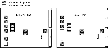
Figure 2: jumper settings for master and slave interface cards. Note also the PQFP configuration.
No software configuration is necessary, although the jumper settings for the two types of card must be set. Figure 2 shows the configuration for a master and a slave unit. The PQFP must also be configured as in the diagram (shaded = present, no shading = removed).
SLOW: $BF'FF00
FAST: $BF'FFE0
FANOUT: $BF'FF80
Trigger-Bit: $BF'F000
The card configurations are illustrated in figure 3. For further information about the software or hardware configurations of the cards, see [6], [7] and [8], and section 3.
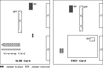
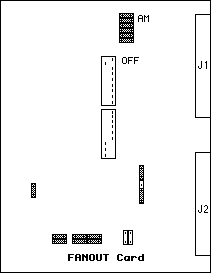
Figure 3: STC Cards configurations.
This section describes the connections required between the various STC modules used in the Silicon Tracker DAQ branch. The wiring refers to the J2 position of the STC cards, which have a 5-row DIN connector. For further documentation of the STC cards, refer to the appropriate manuals ([6], [7], [8]).
The STC cards are arranged as follows: (slots 1-4 are standard VME/VSB)
                Card             Abbreviaton    Slot
                Slow Card             SC         5
                Fast Card             FC         6
                Fanout Card           FO         7
                Trigger-bit           TB         8
                Card
                L2/3 Card            L2L3        9
                Store Card            ST         10
    Signal           Pin        to              Pin             Signal
 L1Kp*           8e                   SC         29b             ScClk1
 L2KpPl          8d                   SC         27b             ScClk2
 FER*            13d                  SC         23b             L2Kp
 Run*            21e                  SC         26b             ScGate2*
 ExtRes*         18e                  SC         11e             PrepRun
 Mode0*          30d                  SC         24b             Mode0*

 PrpRun*         16e                 self        18e             ExtRes*

 PEn-            2e                   FO         2b              PEIn-1
 PEn+            2d                   FO         2a              PEIn+
 HCk-            2b                   FO         2e              HCkIn-
 HCk+            2a                   FO         2d              HCkIn+
 L2KpPl*         22d                  FO         17a             SlowIn*(1)
 FsClr*          7d                   FO         18a             SlowIn*(2)
 FERRrIn         17d                  FO         15d             InSig5*(1)2

 L1Kp*           8e                   TB         8e              L1Kp*
 L2Kp*           11d                  TB         9e              L2Kp*
 MBit0           30e                  TB         4d              MBit0
 MBit1           28e                  TB         5d              MBit1
 Mode4           28d                  TB         6d              Mode4
    Signal           Pin        to              Pin             Signal
 ScClk1          29b                  FC         8e              L1Kp*
 ScClk2          27b                  FC         8d              L2KpPl
 L2Kp            23b                  FC         13d             FER*
 ScGate2*        26b                  FC         21e             Run*
 PrepRun         11e                  FC         18e             ExtRes*
 Mode0*          24b                  FC         30d             Mode0*

 PrepRun         11e                 self        30b             ScalerClr
 ScGate2*        26b                 self        28b             ScGate1*

 INTLOut*0       21b                  FO         16a             SlowIn*(4)
 INTLOut*1       20b                  FO         19a             SlowIn*(3)
    Signal           Pin        to              Pin             Signal
 PEIn-           2b                   FC         2e              PEn-
 PEIn+           2a                   FC         2d              PEn+
 HCkIn-          2e                   FC         2b              HCk-
 HCkIn+          2d                   FC         2a              HCk+
 SlowIn*(1)      17a                  FC         22d             L2KpPl*
 SlowIn*(2)      18a                  FC         7d              FsClr*
 InSig5*(1)      15d                  FC         17d             FERRrIn

 SlowIn*(4)      16a                  SC         21b             INTLOut*0
 SlowIn*(3)      19a                  SC         20b             INTLOut*1

 Fast1-(1)       11e                 L2L3        4b              HCk-
 Fast1+(1)       11d                 L2L3        4a              HCk+
 Fast1-(2)       10e                 L2L3        3b              PEn-
 Fast1+(2)       10d                 L2L3        3a              PEn+
 Slow1-(2)       8e                  L2L3        6b              Abort-
 Slow1+(2)       8d                  L2L3        6a              Abort+
Note: the fanout output from port #5, ie the front cable port, is used as input to the silicon STC interface card. The latter expects the following (where the pin number refers to the F1 connector of the STC bus on the interface card).
    Signal           Pin        Direction       Pin             Signal
 HCK+            3                    in         3               Fast#+(1)
 HCK-            4                    in         4               Fast#-(1)
 PEn+            5                    in         5               Fast#+(2)
 PEn-            6                    in         6               Fast#-(2)
 L2Kp+           7                    in         7               Slow#+(1)
 L2Kp-           8                    in         8               Slow#-(1)
 FsClr+          9                    in         9               Slow#+(2)
 FsClr-          10                   in         10              Slow#-(2)
 L3K+            11                   in         11              Slow#+(3)
 L3K-            12                   in         12              Slow#-(3)
 L3R+            13                   in         13              Slow#+(4)
 L3R-            14                   in         14              Slow#-(4)

 FER+            17                  out         17              InSig#+(1)
 FER-            18                  out         18              InSig#-(1)
    Signal           Pin        to              Pin             Signal
 L1Kp*           8e                   FC         8e              L1Kp*
 L2Kp*           9e                   FC         11d             L2Kp*
 MBit0           4d                   FC         30e             MBit0
 MBit1           5d                   FC         28e             MBit1
 Mode4           6d                   FC         28d             Mode4
    Signal           Pin        to              Pin             Signal
 HCk-            4b                   FO         11e             Fast1-(1)
 HCk+            4a                   FO         11d             Fast1+(1)
 PEn-            3b                   FO         10e             Fast1-(2)
 PEn+            3a                   FO         10d             Fast1+(2)
 Abort+          6a                   FO         8d              Slow1+(2)
 Abort-          6b                   FO         8e              Slow1-(2)
Also wrap the busy daisy chain to the store cards, and the flat wire bus for the PQZP system. 100[[Omega]] pull-up resistors for clock and pipeline enable signals are not necessary for short bus...?
The SiSTC library provides a set of routines to handle signals from the Subsystem Trigger Control (STC) Cards. The library can be linked directly to Assembler, Pascal and C code written within the MPW programming environment, although some manipulation may be required by programmers wishing to link to a THINK C project (see section 3.4). Note that a standalone application for direct access to STC cards from a Macintosh computer is available from the author.
The STC cards receive all signals distributed by the central trigger system, based on the protocol described in [4]. There are several types of STC cards; the Slow Card, Fast Card, Fanout Card and Triggerbit Card. The function of each is described in the appropriate manual, but can be summarised as follows:
1) Fast Card: this receives all signals which change in strict synchronism with the HERA Clock. These signals need to be distributed quickly in parallel to all subsystems, whilst maintaining their phase relationships to each other. Distributed signals include the HERA Clock, Bunch Scalers, Pipeline Enable, L1 Keep, L2 Keep, L1 Active, Fast Clear and Run. Scalers on the fast card need to be read for each event, and are used to tag the event number. Writeable control bits may be set to signal that the hardware has finished processing an event and is ready to accept new events, or this function can be supported by hardware signals. The STC fast card can be used in a standalone mode to generate local trigger sequences.
2) Slow Card: receives signals not requiring fast, synchronised distribution. These include Prepare Run, Terminate Run, L3 Keep and L3 Reject. Other signals are available, but not defined by the central trigger control system at present. The slow card has a programmable vector table for interrupts, and can be configured to generate VMEbus interrupts on levels 4-6. The interrupts can be masked (enabled/disabled), and flip-flops polled instead. Interrupts are acknowledged by setting appropriate registers. The slow card also houses some scalers which have to be read out with each event.
3) Fanout Card: these cards output the internal signals of the STC in NIM and differential form, allowing individual delays and gating of all signals.
4) Triggerbit Card: used for selective readout, depending on which subtrigger bits triggered the event.
* STC Card base addresses
FCBASE EQU $D0BFFFE0 ; Base address of FastCard
SCBASE EQU $D0BFFF00 ; Base address of SlowCard
FOBASE EQU $D0BFFF80 ; Base address of FanoutCard
* FC Write addresses
* --- D32 not supported by STC! Use D16 or D08 --- Reg size
FCCTL EQU FCBASE ; Control Word .W
FCSDFF1I EQU FCBASE+2 ; Scaledown FF1 (inverted) .B
FCSDFF2I EQU FCBASE+3 ; Scaledown FF2 (inverted) .B
FC1ATVDI EQU FCBASE+4 ; Local L1 delay (inverted) .B
FC2DECDI EQU FCBASE+6 ; Local L2 delay (inverted) .W
FCAFERDI EQU FCBASE+8 ; Auto-FER delay (inverted) .W
FCEXEC EQU FCBASE+$D ; Execute Byte .B
* FC Read addresses
FCSTABUN EQU FCBASE ; status bits & bunch scaler .L
FCREVC EQU FCBASE+4 ; revolution counter .L
FCAPXU1 EQU FCBASE+8 ; app crossings upper byte .L
FCAPXL4 EQU FCBASE+$C ; app xings lower 4 bytes .L
FCL1XU1 EQU FCBASE+$10 ; l1atv xings upper byte .L
FCL1XL4 EQU FCBASE+$14 ; l1atv xings lower 4 bytes .L
* FC Execute Byte
FCRESET EQU $30 ; CReset (resets most things) .B
FCSCRES EQU $31 ; Reset scalers .B
FCRESFF EQU $32 ; Reset local L1 FFs .B
FCSETFER EQU $34 ; Set Front-End-Ready .B
FCLL1PR EQU $36 ; Load L1 prescalers 1st time .B
FCAUTO EQU $37 ; Generate auto-sync event .B
FCSTOP EQU $38 ; Stop Run .B
FCSTART EQU $3A ; Start Run .B
* SC write addresses
SCIEN EQU SCBASE ; interrupt enable word .W
SCMSK EQU SCBASE+2 ; interrupt mask word .W
SCCLR EQU SCBASE+4 ; set/clear interrupt .W
*SC Read addresses
SCINST EQU SCBASE ; status of interrupt enable .W
SCMKST EQU SCBASE+2 ; status of masks .W
SCFFST EQU SCBASE+4 ; status of FFs .W
SCOUT EQU SCBASE+6 ; outward info bits .W
SCL1KS EQU SCBASE+8 ; L1K scaler .L
SCL2KS EQU SCBASE+$C ; L2K scaler .L
Initialise all STC cards
Pascal/C : P_STCInit(MODE:longint; IERR:var);
Assembler : STC_INIT D7=MODE, D0(exit)=IERR.
Clears all slow card interrupts, enables interrupts 0-3 (L3R, L3K, Terminate Run and Prepare Run respectively), but masks them so that they do not generate VMEbus interrupts, but can be polled instead. If the mode is non-zero, the STC cards are set-up to run in standalone mode, otherwise the STC cards receive all signals from the Central Trigger Control system.
The possible error codes, IERR, returned are:
$BE = Bus Error accessing STC cards.
0 = No Error.
Read STC scalers
Pascal/C : P_STCReadScalers(SISTORE:longint; IERR:var);
Assembler : STC_READ_SCALERS A2=SISTORE, D0(exit)=IERR.
Reads STC scalers to the address given by the SISTORE argument. The space required is 14 32-bit words. The data are formatted according to the 'TSTC' BOS bank (B32), which is as follows:
NAME='TSTC',DUM1=12(SILICON BRANCH),DUM2=0,LEN32=10,NUM_COL=8,NUM_ROW=1
DATA[8]=NSTBUN,NREV,NXING2,NXING0,NACT2,NACT0,NL1KP,NL2KP.
Note that D32 transfers are not possible to STC cards (use D16 instead), but block transfers are. The routine at present does not use this option, so as to be hardware independent.
The possible error codes, IERR, returned are:
$BA = Bus Error accessing store address.
$BE = Bus Error accessing STC cards.
0 = No Error.
Check for Slow Card Interrupts
Pascal/C : P_STCCheckL3(L3STAT:var);
Assembler : STC_SC_TAS D7(exit)=L3STAT.
Checks the slow card for pending interrupts. Prepare run and terminate run interrupts are acknowledged but not flagged, as these can be handled by polling SYSMODE. Level-3 interrupts are cleared but are also flagged in the return argument. No Bus Error checking is done for speed's sake.
The possible return codes are:
0 = No interrupt pending.
1 = L3R received (and cleared).
2 = L3K received (and cleared).
Bit(s  Description
  )
  0    Clock error during last minute
  1    Clock error now; during READ action
 2-4   Three outward spare signals driven
       by CTC
       (In reverse order, SprOut3 in bit
       2)
  5    Run. ( = 1 if running)
 6+8   The inverse of FER ( = 0 if FER)
  7    PEn, pipelines enabled
  9    L2K
 10    L1K
 11    L1 active
12-15  Local L1 flip-flops 1-4
During a normal run, therefore, the front-end readout sequence (and scaler read) begins as soon as the following bits are set: !FER, Run, L1K and L2K (bit-mask = $0760). We don't check the other signals.
1. Add the .o file to your project.
2. Select the .o Converter options command from the Edit menu.
3. Check both the "use Toolbox trap list" and the "use `.v' file" check boxes.
4. In your project window select your .o file, and choose Compile from the Source menu.
A `vocabulary' file is now created in the same directory as the .o file. That is, a file with the same name as your .o file, but suffixed `.v'. Edit this file changing upper case declarations such that the routines are named with the correct uppercase and lowercase spellings, as above.
Now repeat step 4 above. Refer to [9] for further details.
The SiMac library is intended for programmers who require simple and direct high-level access to OnSiRoC controllers from the Macintosh, where the user does not have access to a VMEtaxi module. The library is an extension to the basic driver primitives described in [1].
The library routines are called with much the same syntax as SiUSER routines, although the VMEtaxi -- Macintosh command address parameter is omitted. SiMac instead assumes that the OnSiRoC has a pre-defined, fixed base address[+]. The library can be linked directly to Assembler, Pascal and C code written within the MPW programming environment, although some manipulation may be required by programmers wishing to link to a THINK C project (see section 3.4).
ADDERR : Address where error found.
CCPIC1 : Channel + Pipeline Counter 1.
CCPIC2 : Channel + Pipeline Counter 2.
CDTHRESH : Cluster Detector Threshold.
DATAREAD : Data Read. Only valid when returned error code is non-zero.
DATASENT : Data Sent / written. Only valid when returned error code is non-zero.
HDTHRESH : Hit Detector Threshold.
IERR : Integer Error Code.
NEXTADD : Next Address. Used when loading pedestals or reading data from consecutive OnSiRoCs. Only valid when returned error code is zero.
NEXTCC : Next value of CCPIC1.
NUMREAD : Number of 32-bit words read. i.e. number of hits, pulses or clusters found.
SICC1 : Channel Counter 1.
SICC2 : Channel Counter 2.
SICDTHR : Cluster Detector Threshold.
SICTRLR1 : Control Register 1.
SICTRLR2 : Control Register 2.
SICURR1 : Current 1.
SICURR2 : Current 2.
SICURR3 : Current 3.
SICURR4 : Current 4.
SIHDTHR : Hit Detector Threshold.
SILLPULS : Length to left of cluster pulse.
SILRPULS : Length to right of cluster pulse.
SINUM : OnSiRoC Number.
SIPIC : Pipeline Counter.
SIROCPAT : Bit pattern of OnSiRoCs found.
SISEED : Random Number seed used for creating reproducible random number sequences.
SISTAT : OnSiRoC Status Register.
SISTORE : Store Address. Any contiguous VME memory area used to store sequencer and pedestal values, and destination address for writing to.
SIVOLT1 : Bias Voltage 1.
SIVOLT2 : Bias Voltage 2.
SIVOLT3 : Bias Voltage 3.
SIVOLT4 : Bias Voltage 4.
Initialise all OnSiRoCs in a crate
Pascal/C : P_SIinitA(SIROCPAT:var);
Assembler : SI_ALL_INIT D7(exit)=SIROCPAT.
There are no return error codes for this routine.
Initialise OnSiRoC
Pascal/C : P_SIinit(SINUM:longint; IERR:var);
Assembler : SI_INIT D7=SINUM, D0(exit)=IERR.
The possible error codes, IERR, returned are:
$FF = Invalid OnSiRoC number.
$BE = Bus Error accessing OnSiRoC.
0 = No Error.
Get OnSiRoC Status
Pascal/C : P_SIstat(SINUM:longint; SISTAT, CCPIC1, CCPIC2, HDTHRESH, CDTHRESH, IERR:var);
Assembler : SI_STAT D7=SINUM, D5(exit)=CDTHRESH, D4=HDTHRESH, D3=CCPIC2, D2=CCPIC1, D1=SISTAT, D0=IERR.
The possible error codes, IERR, returned are:
$FF = Invalid OnSiRoC number.
$BE = Bus Error accessing OnSiRoC.
0 = No Error.
Set Bias Voltages
Pascal/C : P_SIvolts(SINUM, SIVOLT1, SIVOLT2, SIVOLT3, SIVOLT4:longint; IERR:var);
Assembler : SI_SET_VOLTS D7=SINUM, D4=SIVOLT4, D3=SIVOLT3, D2=SIVOLT2, D1=SIVOLT1, D0(exit)=IERR.
The possible error codes, IERR, returned are:
$FF = Invalid OnSiRoC number.
$BE = Bus Error accessing OnSiRoC.
0 = No Error.
$02 = Invalid Setting.
Read Currents
Pascal/C : P_SIcurr(SINUM:longint; SICURR1, SICURR2, SICURR3, SICURR4, IERR:var);
Assembler : SI_READ_CURRENT D7=SINUM, D4(exit)=SICURR4, D3=SICURR3, D2=SICURR2, D1=SICURR1, D0=IERR.
The possible error codes, IERR, returned are:
$FF = Invalid OnSiRoC number.
$BE = Bus Error accessing OnSiRoC.
0 = No Error.
Set Control Registers
Pascal/C : P_SIctrl(SINUM, SICTRLR1, SICTRLR2:longint; IERR:var);
Assembler : SI_CTRL D7=SINUM, D2=SICTRLR2, D1=SICTRLR1, D0(exit)=IERR.
The possible error codes, IERR, returned are:
$FF = Invalid OnSiRoC number.
$BE = Bus Error accessing OnSiRoC.
0 = No Error.
Set Channel and Pipeline Counters
Pascal/C : P_SIccpic(SINUM, SICC1, SICC2, SIPIC:longint; IERR:var);
Assembler : SI_CCPIC D7=SINUM, D4=SIPIC, D2=SICC2, D1=SICC1, D0(exit)=IERR.
The possible error codes, IERR, returned are:
$FF = Invalid OnSiRoC number.
$BE = Bus Error accessing OnSiRoC.
0 = No Error.
$01 = Counters not set OK
Set Thresholds
Pascal/C : P_SIthresh(SINUM, SIHDTHR, SICDTHR:longint; IERR:var);
Assembler : SI_THRESH D7=SINUM, D5=SICDTHR, D4=SIHDTHR, D0(exit)=IERR.
The possible error codes, IERR, returned are:
$FF = Invalid OnSiRoC number.
$BE = Bus Error accessing OnSiRoC.
0 = No Error.
$03 = Hit Detector Threshold not set OK
$0C = Cluster Detector Threshold not set OK
$0F = Hit and Cluster Detector Thresholds not set OK
Load Sequencer
Pascal/C : P_SIloadSEQ(SINUM, SISTORE:longint; IERR:var);
Assembler : SI_LOAD_SEQ A1=SISTORE, D7=SINUM, D0(exit)=IERR.
The possible error codes, IERR, returned are:
$FF = Invalid OnSiRoC number.
$BE = Bus Error accessing OnSiRoC.
$BA = Bus Error finding store.
0 = No Error.
Check Sequencer
Pascal/C : P_SIcheckSEQ(SINUM, SISTORE:longint; ADDERR, DATASENT, DATAREAD, IERR:var);
Assembler : SI_CHECK_SEQ A1=SISTORE, D7=SINUM, A0(exit)=ADDERR, D4=DATAREAD, D3=DATASENT, D0=IERR.
The possible error codes, IERR, returned are:
$FF = Invalid OnSiRoC number.
$BE = Bus Error accessing OnSiRoC.
$BA = Bus Error finding store.
$CF = Check Failure.
0 = No Error.
Load Pedestals
Pascal/C : P_SIloadPED(SINUM, SISTORE:longint; NEXTADD, IERR:var);
Assembler : SI_LOAD_PED A1=SISTORE, D7=SINUM, A1(exit)=NEXTADD, D0=IERR.
The possible error codes, IERR, returned are:
$FF = Invalid OnSiRoC number.
$BE = Bus Error accessing OnSiRoC.
$BA = Bus Error finding store.
0 = No Error.
Check Pedestals
Pascal/C : P_SIcheckPED(SINUM, SISTORE:longint; ADDERR, DATASENT, DATAREAD, NEXTADD, NEXTCC, IERR:var);
Assembler : SI_CHECK_PED A1=SISTORE, D7=SINUM, A1(exit)=NEXTADD, A0=ADDERR, D4=DATAREAD, D3=DATASENT, D1=NEXTCC, D0=IERR.
The possible error codes, IERR, returned are:
$FF = Invalid OnSiRoC number.
$BE = Bus Error accessing OnSiRoC.
$BA = Bus Error finding store.
$CF = Check Failure.
0 = No Error.
Read Hits
Pascal/C : P_SIreadHITS(SINUM, SISTORE:longint; NUMREAD, NEXTADD, IERR:var);
Assembler : SI_READ_HITS A2=SISTORE, D7=SINUM, A2(exit)=NEXTADD, D6=NUMREAD, D0=IERR.
The possible error codes, IERR, returned are:
$FF = Invalid OnSiRoC number.
$BE = Bus Error accessing OnSiRoC.
$BA = Bus Error finding store.
$11 = Invalid Pointer Counter value.
0 = No Error.
With this routine only the pointer memory is read out and transferred to the data store. The readout sequence follows the 3-1-4-2 channel sequence of the OnSiRoC.
Read Data
Pascal/C : P_SIreadDATA(SINUM, SISTORE:longint; NUMREAD, NEXTADD, IERR:var);
Assembler : SI_READ_DATA A2=SISTORE, D7=SINUM, A2(exit)=NEXTADD, D6=NUMREAD, D0=IERR.
The possible error codes, IERR, returned are:
$FF = Invalid OnSiRoC number.
$BE = Bus Error accessing OnSiRoC.
$BA = Bus Error finding store.
$11 = Invalid Pointer Counter value.
$22 = Invalid Cluster size.
$77 = Invalid Raw Data.
0 = No Error.
This routine reads out the hits and cluster data before transferring to the data store. The readout sequence follows the 3-1-4-2 channel sequence of the OnSiRoC.
Read Pulses
Pascal/C : P_SIreadPULSE(SINUM, SISTORE, SILLPULS, SILRPULS:longint; NUMREAD, NEXTADD, IERR:var);
Assembler : SI_READ_PULSE A2=SISTORE, D7=SINUM, D4=SILRPULS, D3=SILLPULS, A2(exit)=NEXTADD, D6=NUMREAD, D0=IERR.
The possible error codes, IERR, returned are:
$FF = Invalid OnSiRoC number.
$BE = Bus Error accessing OnSiRoC.
$BA = Bus Error finding store.
$E1 = Invalid length of pulse requested.
$11 = Invalid Pointer Counter value.
$22 = Invalid Cluster size.
$77 = Invalid Raw Data.
$27 = Invalid length counter because of bad pointer memory value.
0 = No Error.
This is the same as SI_READ_DATA but allows for a specified pulse length in software.
Read Raw Data
Pascal/C : P_SIreadRAW(SINUM, SISTORE:longint; NEXTADD, IERR:var);
Assembler : SI_READ_RAW A2=SISTORE, D7=SINUM, A2(exit)=NEXTADD, D0=IERR.
The possible error codes, IERR, returned are:
$FF = Invalid OnSiRoC number.
$BE = Bus Error accessing OnSiRoC.
0 = No Error.
This routine transfers all raw memory data to the store, ie 4096 32-bit words. The readout sequence follows the 3+1 - 4+2 channel pairs of the OnSiRoC.
Test Sequencer Memory
Pascal/C : P_SItestSEQ(SINUM, SISEED:longint; DATASENT, DATAREAD, IERR:var);
Assembler : SI_TEST_SEQ D7=SINUM, D6=SISEED, D6(exit)=NEXTSEED, D4=DATAREAD, D3=DATASENT, D0=IERR.
The possible error codes, IERR, returned are:
$FF = Invalid OnSiRoC number.
$BE = Bus Error accessing OnSiRoC.
$CF = Check Failure.
0 = No Error.
Test Pedestal Memory
Pascal/C : P_SItestPED(SINUM, SISEED:longint; DATASENT, DATAREAD, NEXTCC, IERR:var);
Assembler : SI_TEST_PED D7=SINUM, D6=SISEED, D6(exit)=NEXTSEED, D4=DATAREAD, D3=DATASENT, D1=NEXTCC, D0=IERR.
The possible error codes, IERR, returned are:
$FF = Invalid OnSiRoC number.
$BE = Bus Error accessing OnSiRoC.
$C1 = Invalid CC1. CC1 not incremented correctly.
$CF = Check Failure.
0 = No Error.
Test Pointer Memory
Pascal/C : P_SItestPOINT(SINUM, SISEED:longint; ADDERR, DATASENT, DATAREAD, NEXTCC, IERR:var);
Assembler : SI_TEST_POINT D7=SINUM, D6=SISEED, A2(exit)=ADDERR, D6=NEXTSEED, D4=DATAREAD, D3=DATASENT, D1=NEXTCC, D0=IERR.
The possible error codes, IERR, returned are:
$FF = Invalid OnSiRoC number.
$BE = Bus Error accessing OnSiRoC.
$C0 = Invalid PC. Pointer Counter not incremented correctly.
$C2 = Invalid CC2. CC2 not incremented correctly.
$CF = Check Failure.
0 = No Error.
Test Raw Data Memory
Pascal/C : P_SItestRAW(SINUM, SISEED:longint; ADDERR, DATASENT, DATAREAD, NEXTCC, IERR:var);
Assembler : SI_TEST_RAW D7=SINUM, D6=SISEED, A2(exit)=ADDERR, D6=NEXTSEED, D4=DATAREAD, D3=DATASENT, D1=NEXTCC, D0=IERR.
The possible error codes, IERR, returned are:
$FF = Invalid OnSiRoC number.
$BE = Bus Error accessing OnSiRoC.
$C2 = Invalid CC2. CC2 not incremented correctly.
$CF = Check Failure.
0 = No Error.
SiTest is a stand-alone application which allows the user to perform basic I/O tests of OnSiRoC controllers from a Macintosh computer. It also provides a user friendly interface from which to execute SiMac primitives described in section 4, and further in [1]. As with the SiMac library, SiTest assumes that the OnSiRoC has a pre-defined, fixed base address in VME.
* Menu-selectable OnSiRoC register offsets.
* SiMac primitives interface and execution.
* Loading sequencer & pedestal memories.
* Text file <-> raw data file conversion.
* Write events from OnSiRoC memories to files on the Mac.
Planned:
* FTP facility to log events to other devices.
* Full pedestal -> FADC -> raw data calibration chain.
* Pattern editor for FADC calibration files (# successive pulses, amplitude etc.).
* Sequencer compiler/editor interface.
* Complete hardware tests and diagnostics.
Other points of interest are:
* When reading or writing with the loop option set, exit by pressing the mouse button.
* The data box is only editable when the `write' option is selected.
*`Byte', `Short' and `Long' correspond to 8-bit, 16-bit and 32-bit data respectively.
* All values used are saved as defaults on exiting SiTest.
To use, select an OnsiRoC primitive from the pop-up menu, change the input parameters to the desired values, and press the `Do It' button to execute. Other points of interest are:
* If the Store address is a non-VME address, the user is prompted to Read/Write from/to a Macintosh file. Bear in mind the possible large data volumes involved in reading data from the OnSiRoCs...
* Only raw data files may be downloaded to the OnSiRoCs. These files are suffixed `.si'. Note that a file converting facility is also provided to change TEXT files to raw data format, and vice-versa. See below for more details. Files created by SiTest are raw data files, and to be viewed need to be converted to TEXT files.
* All values used are saved as defaults on exiting SiTest.
* As well as hexadecimal input values for setting the bias voltages, the user may also set the decimal value in the "Power Supplies" window. To select the window if it is not visible, select it from the `Window' menu.
1. Text files must be named filename.txt, and be of type `TEXT'. This means that MPW, TeachText, THINK C files are OK, but Microsoft Word files may not be (Word files are usually saved as formatted `Word Bundles (WDBN)'). Please ensure that there are no trailing spaces after the last data word! Text files which are converted to raw data files are named filename.si.
2. Raw data files are named filename.si. They are converted to THINK C text files, but may be viewed with any text editor.
This section is intended as a guide to processes relying on the farm for communicating with the silicon data acquisition branch. Such processes include slow control tasks, detector control tasks, and any other process serving silicon control or monitoring purposes. This is necessary because the only access to front-end electronics, including detector control electronics, is through the data acquisition chain.
Three slow control tasks are currently identified. They can be loosely categorised as serving the CST, BST (pad and strips) and the Radiation Monitor. Each of these tasks (running on Macintosh computers) currently has access to shared memory in the silicon farm crate. The memory is split amongst the tasks as follows, where each task can use up to 128 kBytes of memory for whatever purpose they require:
                      Task                  A24 base address
                      CST                   C0'0000
                      BST                   C2'0000
                      RadMon                C4'0000
The first 64 bytes of each task area is reserved for inter-processor communication. This header block is used as follows, where each variable is a 32-bit integer:
                      Offset                Variable
                      $00                   Command
                      $04                   Response
                      $08                   Address
                      $0C                   Length
                      $10                   Watchdog
                      $14-$3C               Reserved
Some of the commands detailed below act directly on front-end hardware, whereas others are used to update the stored default values to be loaded when the system is initialised, i.e. when crates are powered on, or at a later time as invoked by additional commands. Note also that there is a distinction in the OnSiRoC between setting the bias voltage values and actually turning the bias voltages on.
The following control and monitoring commands are handled by the farm co-ordinating task:
* Read currents of a single OnSiRoC;
* Feed data back into the data-stream;
* Set the bias values of one OnSiRoC. This command does not update the stored default value;
* Update (write) all stored default bias values;
* Request (read) all stored default bias values;
* Set the bias voltages of several OnSiRoCs in a single crate with their default values;
* Switch on/off the power supplies of several OnSiRoCs;
* Request the 'perceived' state of all power supplies.
The description of the latter command raises an important point; the actual status of power supplies and the magnitude of their settings cannot be determined in the present system. Instead the status is inferred from whether commands returned error codes or not i.e. if no error is returned, it is assumed that the status of the voltages supplied to the detectors is that requested by the slow control task!
As there is no direct-access to front-end crates, many commands require arguments specifying the remote crate number and an OnSiRoC number. At present the CST crate is crate number one, with the BST in crates 2 and 3. Additional arguments are defined in the command description below. Note that the examples use the CST slow control task offset, all arguments are 32-bit integers, and that the commands syntax is that of VME_Tools executed from the MPW Shell [10].
The communication protocol is the following: the command is set by the slow control task, additionally setting the length variable if appropriate. Where extra input arguments are required by particular commands, the address variable is used as an offset to those arguments. The address variable is also used to indicate where return arguements are to be written. On completion of the command, the command variable is set to zero, and the response variable set; this will be zero if the action was completed successfully, else it will be an error code. For commands which request data to be written to the slow control's memory area, the length variable is also set after successfully completing a command. The watchdog variable is cleared each time the slow control tasks are polled.
Description: Reads the currents of each of the four bias power supplies in a single OnSiRoC.
Input Arguments: Argument offset, taxi number, OnSiRoC number.
Return Arguments: Response, length, currents 1-4. Note that although the arguments returned are always 32-bit integers, current values are 16-bit words (mask off upper 16-bits).
Example: MM $xxC00008 $00000040 -L ; # Set address to arguments' offset
MM $xxC00040 $00000001 -L ; # CST crate (1)
MM $xxC00044 $00000000 -L ; # OnSiRoC 0
MM $xxC00000 $00000326 -L ; # Set command
Wait for completion (command set back to zero), and if the response variable is zero (no error) the currents will be written to the address offset pointed to by the address argument.
Description: Sends data to be included in the data stream. Note that this is not possible when a run is not in progress.
Input Arguments: Data offset, length of data (bytes).
Return Arguments: Error returned indicates that run is not in progress ($99), that the data size is too large ($22), or try again (-1).
Example: MM $xxC00008 $00000040 -L ; # Set address to data offset
MM $xxC0000C $00000400 -L ; # 1 kByte
MM $xxC00000 $0000FEED -L ; # Set command
Wait for completion (command set back to zero), and check response variable.
Description: Sets the bias values of the four bias power supplies in a single OnSiRoC. This command does not actually switch the power supplies on or off.
Input Arguments: Argument offset, taxi number, OnSiRoC number, bias values 1-4.
Return Arguments: Response.
Example: MM $xxC00008 $00000040 -L ; # Set address to arguments' offset
MM $xxC00040 $00000001 -L ; # CST crate (1)
MM $xxC00044 $00000000 -L ; # OnSiRoC 0
MM $xxC00048 $00000010 -L ; # Bias 1
MM $xxC0004C $00000020 -L ; # Bias 2
MM $xxC00050 $00000030 -L ; # Bias 3
MM $xxC00054 $00000040 -L ; # Bias 4
MM $xxC00000 $00000325 -L ; # Set command
Wait for completion (command set back to zero), and if the response variable is zero (no error) the values were set.
Description: Stores the bias values of all OnSiRoCs as default settings. This should be the default command for HV control, together with set multiple bias values, and switch power supplies ON/OFF.
Input Arguments: Argument offset, 320-byte block containing bias settings of all OnSiRoCs. The block is arranged as follows: bias settings 1-4 (4 16-bit words) for 16 OnSiRoCs in CST crate, 16 OnSiRoCs in BST crate 1, and 8 OnSiRoCs in the second BST crate.
Return Arguments: Response
Example: MM $xxC00008 $00000040 -L ; # Set offset of data block
MM 320-byte block of all settings
MM $xxC00000 $00000100 -L ; # Set command
Wait for completion (command set back to zero), and if the response variable is zero (no error) the default settings are stored. These can be checked later with request default bias values.
Description: Reads back the default settings of all OnSiROC bias values.
Input Arguments: Offset to return storage area.
Return Arguments: Response and length of data returned.
Example: MM $xxC00008 $00000040 -L ; # Set address to data offset
MM $xxC00000 $00000101 -L ; # Set command
Wait for completion (command set back to zero), and check response variable. If zero, data at the offset address will contain all default bias settings.
Description: Sets the stored default bias settings of up to 16 OnSiRoCs in a single front-end crate.
Input Arguments: Argument offset, taxi number, OnSiRoC mask.
Return Arguments: Response.
Example: MM $xxC00008 $00000040 -L ; # Set address to arguments' offset
MM $xxC00040 $00000001 -L ; # CST crate (1)
MM $xxC00044 $0000010F -L ; # OnSiRoC mask (0-3 and 8)
MM $xxC00000 $0000032B -L ; # Set command
Wait for completion (command set back to zero), and check response variable. If zero, all values were set correctly.
Description: Switches the power supplies ON or OFF for up to 16 OnSiRoCs in a single front-end crate. Due to a quirk of the OnSiRoC design, all power supplies (analogue, digital and bias) have to be set at the same time. If the command does not return an error, the 'state' of the power supplies is also stored.
Input Arguments: Argument offset, taxi number, OnSiRoC mask, 32-byte block of masked state of all power supplies in a crate. The block is organised as follows: 16 16-bit words of bit packed power supply status. In each word bits 0-3 set the analogue supply of channels 1-4, bits 4-7 the digital supply, and bits 8-11 the bias supply. The signals are active low i.e. set the bit to zero if the coresponding supply is to be switched ON (1=off). For more information refer to a description of the OnSiRoC control register 2 (section 1).
Return Arguments: Response.
Example: MM $xxC00008 $00000040 -L ; # Set address to arguments' offset
MM $xxC00040 $00000001 -L ; # CST crate (1)
MM $xxC00044 $0000010F -L ; # OnSiRoC mask (0-3 and 8)
MM 32-byte block of masks of all power supply status
MM $xxC00000 $0000032A -L ; # Set command
Wait for completion (command set back to zero), and check response variable. If zero, all values were set correctly and the 'status' of the supplies is stored.
Description: Reads back the perceived state of all OnSiROC power supplies. This is not a safe way of checking whether power supplies are ON or OFF (this is not possible with the present OnSiRoC design).
Input Arguments: Return storage area offset.
Return Arguments: Response and length of data returned.
Example: MM $xxC00008 $00000040 -L ; # Set address to data offset
MM $xxC00000 $00000201 -L ; # Set command
Wait for completion (command set back to zero), and check response variable. If zero, data at the offset address will contain all state of all OnSiRoC supplies in bit-packed format as described above.
[1] W. J. Haynes. SiVMEXI. H1 Silicon Trackers: VMEtaxi Data Acquisition. Version 2.3, 27th Sept 1994.
[2] W. Zimmermann. OnSiRoC VME Controller. DESY, 2nd May 1994.
[3] S. Prell. Sequencer compiler for OnSiRoC. DESY, 1994 (in preparation).
[4] H. Krehbiel. The H1 trigger control system. H1-12/88-101, DESY, 1989.
[5] W. Zimmermann. STC Interface Master/Slave Unit. DESY, 20th Jan 1994.
[6] H Krehbiel. The Fast Card of the Subsystem Trigger Controller. DESY, 4th Sept 1990.
[7] J. Olszowska. The Slow Card of the Subsytem Trigger Controller. DESY, 31st Aug 1990.
[8] H. Krehbiel. The Extended Fanout Card of the H1 STC. DESY, 31st July 1991.
[9] Symantec. THINK C: C Development Environment for Macintosh (User's Guide). Version 6, Symantec Corporation, 1993.
[10] W. J. Haynes. VM E_TOOLS, VMEbus interaction from the MPW shell. Version 3.2, DESY, Feb. 1994.
The sequencer register map is reproduced here alphabetically for reference.
Register                             Offset        Length        Read      Write
Bias Voltage/Current 1                 90            .W            x       x
Bias Voltage/Current 2                 92            .W            x       x
Bias Voltage/Current 3                 94            .W            x       x
Bias Voltage/Current 4                 96            .W            x       x
Card Reset with registers 1+2          84            .W                    x
Card Reset without registers1+2        8A            .W                    x
Channel + Pipeline Counter 2           28            .L            x       x
Channel + Pipeline Counter Reset       D6            .W                    x
Channel + Pipeline Countr1             C8            .L            x       x
Channel Counter 1 + 2 Reset            D0            .W                    x
Channel Counter 1 Increment            D2            .W                    x
Channel Counter 1 Reset                CC            .W                    x
Channel Counter 2 Increment            2C            .W                    x
Channel Counter 2 Reset                CE            .W                    x
Clock Divider Reset                    74            .W                    x
Clock Loop Start                       70            .W                    x
Clock Loop Stop                        72            .W                    x
Cluster Detector Threshold             52            .W            x       x
Coarse Pedestal 1                      98            .W            x       x
Coarse Pedestal 2                      9A            .W            x       x
Coarse Pedestal 3                      9C            .W            x       x
Coarse Pedestal 4                      9E            .W            x       x
Control Register 1                     06            .W                    x
Control Register 2                     04            .W                    x
Cosmic Prestart                        DA            .W                    x
Cosmic Start                           DC            .W                    x
Cosmic Stop                            D8            .W                    x
Enable Sequencer                       1E            .W                    x
FADC 1 + 3                             10            .L            x
FADC 2 + 4                             14            .L            x
FADC Clock 1+2+3+4                     3C            .W                    x
Fast Clear                             76            .W                    x
Front-Ends Ready Reset                 7E            .W                    x
Hit Detector Reset 1 + 2               4C            .W                    x
Hit Detector Reset 1+2+3+4             50            .W                    x
Hit Detector Reset 3 + 4               4E            .W                    x
Hit Detector Set + Clock               48            .L                    x
Hit Detector Threshold                 40            .L            x       x
Hit Detector Width                     46            .W            x
Interrupt Test                         F0            .W                    x
Interrupter Clear                      82            .W                    x
Interrupter Set                        80            .W                    x
L2-Delay Reset                         7C            .W                    x
L2-Keep                                78            .W                    x
L2-Reject                              7A            .W                    x
Register                             Offset        Length        Read      Write
L3 Keep, Reject                        FC            .L                    x
Pedestal DAC Clock                     68            .W                    x
Pedestal Memory 1+2+3+4                20            .L            x       x
Pedestal Memory CC1 Increment          24            .L            x       x
Pedestal Memory PIC Increment          C0            .L            x       x
Pipeline Counter Increment             2E            .W                    x
Pipeline Counter Reset                 D4            .W                    x
Pointer + Raw Mem 1 + Inc CC2          AC            .L            x
Pointer + Raw Mem 2 + Inc CC2          B0            .L            x
Pointer + Raw Mem 3 + Inc CC2          B4            .L            x
Pointer + Raw Mem 4 + Inc CC2          B8            .L            x
Pointer Counter 1 + 3                  54            .L            x       x
Pointer Counter 2 + 4                  58            .L            x       x
Pointer Counter Increment 1 + 2        5C            .W                    x
Pointer Counter Increment 1+2+3+4      60            .W                    x
Pointer Counter Increment 3 + 4        5E            .W                    x
Pointer Counter Reset 1 + 2            62            .W                    x
Pointer Counter Reset 1+2+3+4          66            .W                    x
Pointer Counter Reset 3 + 4            64            .W                    x
Pointer Memory 1 + 3                   E8            .L            x       x
Pointer Memory 1 + 3 PC Inc            E0            .L            x       x
Pointer Memory 2 + 4                   EC            .L            x       x
Pointer Memory 2 + 4 PC Inc            E4            .L            x       x
Raw Data Mem 1 + 3 CC2 inc from        A0            .W                    x
FADC
Raw Data Mem 2 + 4 CC2 inc from        BC            .W                    x
FADC
Raw Data Mem 2 + 4 CC2 Increment       A8            .L            x       x
Raw Data Mem 2 + 4 from FADC           F8            .L                    x
Raw Data Memory 1 + 3                  08            .L            x       x
Raw Data Memory 1 + 3 CC2 Inc          A4            .L            x       x
Raw Data Memory 1 + 3 from FADC        F4            .L                    x
Raw Data Memory 2 + 4                  0C            .L            x       x
Sequencer Address 1 + 2                34            .L                    x
Sequencer Address 3                    38            .W                    x
Sequencer Clock                        3A            .W                    x
Sequencer High Memory                  6C            .L                    x
Sequencer Low Memory                   30            .L            x       x
Status Register                        C6            .W            x